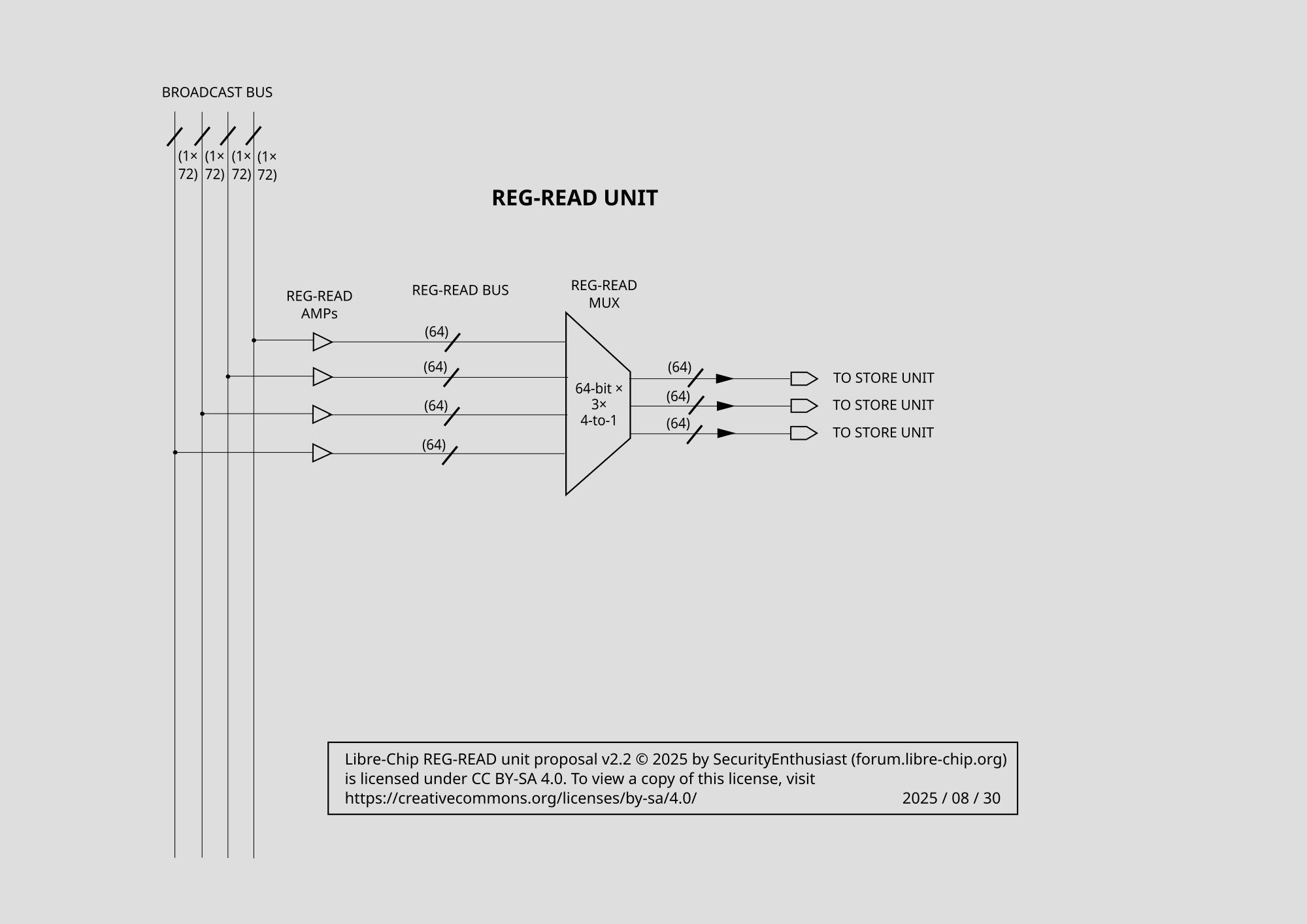
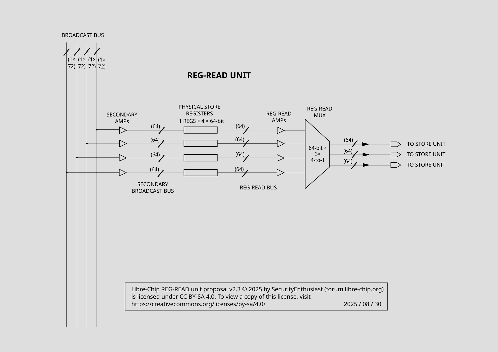
Idea for changing the register file and muxing to make it faster

I have figured out the solution:

For implementing operand registers, we can use both BRAMS and LUTs simultaneously, on the same FPGA chip.

Basically, we implement operand registers with BRAMS that are not used by more important stuff.
When we run out of BRAMs, we use LUTs.

That effectively reduces the number of required LUTs, without compromising availability of BRAMs for implementing other units.

It would work especially well if the speed of the BRAM register files is about the same as the speed of LUT register files.
Such assumption is likely true for register file sizes we need (about 32 registers per file).

After the PowerISA is translated to the internal μOps, there are explicit flag register operands that are register-renamed and are treated just like any other register operand, the only difference is the unit uses the 8 flag bits instead of the 64 data bits and ignores the rest.
Immediates and other instruction fields are not counted as register operands.

It does have 3 input register instructions: mul-add instructions as well as some SIMD instructions. it has both integer and floating-point mul-adds.

In the code I just call them physical registers -- and that term doesn't include the L2 registers.

The original is actually this file which I made with Dia, which is translated to SVG in CI.

The forum is not for documentation, it's for discussion. Documentation should end up on the website or in the source code. The website uses mdBook which is specifically designed for documentation, it's what Rust uses for some of their documentation.
Please don't use the GFDL, since it's incompatible with the LGPL licenses, which means if we added your redone image under the GFDL, we can't copy stuff from it into our other git repositories which are under the LGPL, or copy stuff the other way around if we need to update the image.

Thank you for working on that! Unfortunately our current grant doesn't have any budget specifically for documentation, so you won't get paid for that, but if you like you can look through the task list and see if any of them look interesting -- I'd suggest starting small. If you want to work on one of the tasks, we can almost certainly[1] get you added to the NLnet grant so you can get paid by NLnet for completing those tasks.

The ECP5 LFE5UM-85 has 208 (they call them sysMEM blocks).


  1. IIRC NLnet has trouble paying people in Russia, Iran, and North Korea, but if you live almost anywhere else it shouldn't be a problem. ↩︎

Sorry, I didn't read your reply yet.
I just want to quickly report that I got these number for ALU sizes on FPGa:

	Power ISA integer execution unit:  
		- small, 1 ALU:       15 K LUT4  
		- fast,  1 ALU:       25 K LUT4
	    - multi-alu, small:   30 K LUT4
		- multi-alu, fast:    60 K LUT4

So, I guess that Libre-Chip should initially target an implementation with about 30 K LUT4. Then later, speed can be improved.

To that 30 K LUT4 you have to add another 10 K LUT4 for the register unit and other parts of the execution unit.
So, 40 K LUT4 for the execution unit.

That leaves us about 43 K for the rest on the smallest FPGa. Looks doable.
Just wanted to quickly report the rough estimates.

uses the 8 flag bits instead of the 64 data bits and ignores the rest

Ah — that's the catch: "ignores."
I was getting suspicious about how those merged flags work.

This is a problem: it's a poor design that will waste roughly a third of our physical registers.

Why not store flags in separate registers implemented with LUTs? That should only require about 2,000 LUTs. I don't see any reason why that simple, obvious design wouldn't be used.

It does have 3 input register instructions: mul-add instructions as well as some SIMD instructions. it has both integer and floating-point mul-adds.

I may be mistaken — I’ve never worked with Power ISA.
My understanding:

  • Power ISA v2 does not define a scalar integer fused multiply‑accumulate (MAC).
  • SIMD (AltiVec/VMX) is a separate unit with its own vector registers; it does not use scalar GPRs.

Also, this thread is about drawing and discussing just the integer execution unit. Other units are not planned in Libre-Chip until later.

In the code I just call them physical registers -- and that term doesn't include the L2 registers.

I’d call L2 registers part of the physical register set, following common terminology.

What you label as “physical registers” (and sometimes “input registers” or “output registers”) I’d call operand registers. Using “physical registers” for those is misleading.

The original is actually this file which I made with Dia, which is translated to SVG in CI.

Misunderstanding... my original drawing is an SVG file.

Please don't use the GFDL, since it's incompatible with the LGPL licenses, which means if we added your redone image under the GFDL, we can't copy stuff from it into our other git repositories which are under the LGPL, or copy stuff the other way around if we need to update the image.

I ran into that same GFDL/LGPL compatibility issue yesterday — it’s a tricky topic and we should discuss it separately. For now: the images I’ve posted so far are licensed CC‑BY‑SA 4.0, which is compatible with the GPL used by Libre‑Chip GIT.

Thank you for working on that! Unfortunately our current grant doesn't have any budget specifically for documentation, so you won't get paid for that,

That’s fine — I’ll do it for free.

you can look through the task list and see if any of them look interesting -- I'd suggest starting small.

I had a quick glance. I think I can do this:

€ 2000 Issue #12 Create the PowerISA decoder

Plan: produce overview diagrams, then implement the decoder (C++, or Python/JavaScript if preferred).

I'm fairly busy, so I can only start later — estimate: delivery in about 6 months. If someone else finishes it before I do, feel free to award them the grant.

The ECP5 LFE5UM-85 has 208 (they call them sysMEM blocks).

Ah — that's the catch. In that case the operand registers will be BRAMs.

Anyway, can we finally:
a) Select a reasonable name for "operand registers"?
b) Select a reasonable target number of operand registers overall, or "operand registers" per unit? I know it's configurable, but I need a concrete target to put in the schematic — that makes it easier to understand.
c) Decide whether we should use two banks for the L2 register file.

Also: I strongly recommend implementing a separate register file for flags.

I got you another quick estimate. It is in NAND2 gate equivalents. To convert to LUT4 equivalents, divide the counts by 2.8.

            25 FO4    64-bit inc = 1200 gates    64-bit adder =  3000 gates
            20 FO4    64-bit inc = 1560 gates    64-bit adder =  4500 gates
            15 FO4    64-bit inc = 2100 gates    64-bit adder =  7000 gates
            11 FO4    64-bit inc = 3100 gates    64-bit adder = 10500 gates
            10 FO4    64-bit inc = 3400 gates    64-bit adder = 12500 gates
             9 FO4    64-bit inc = 3800 gates    64-bit adder = 18000 gates
             8 FO4    64-bit inc = 4400 gates

Edit: I forgot to add normalization references:

            FO1 INVERTER     = 0.4 FO4
            FO4 INVERTER     = 1.0 FO4
            FO1 NAND2        ≈ 0.7 FO4
            FO1 half-adder   ≈ 1.0 FO4  (carry)
            FO1 full-adder   ≈ 2.0 FO4  (carry)

reordered my replies somewhat to hopefully make it easier to read.

I do not call L2 registers physical registers because they behave very differently than physical registers in a traditional register-renaming CPU design -- you can't read/write them directly except in special L2 read/write instructions (inserted by the register renamer when any unit runs out of registers, or when it renames a μOp register that is currently only stored in a L2 register).

On architectures like x86 (which I'm designing the CPU to support as part of a later grant), almost every instruction sets flags, so having those flags as part of the same register the output is written to means we only ever have to track one renamed output per instruction, which simplifies the control logic quite a bit since it only requires one kind of register as well as needing quite a few less registers because physical registers are allocated for instructions' outputs, not inputs, so if we didn't have flags and data in the same register then each instruction would need 2 output physical registers allocated for it.

Also, for FPGAs, since their SRAM blocks are generally 9 \times 2^n bits wide, putting an extra 8 bits in the same register as the 64-bits of data is a small additional cost since the minimum width that fits the data is 72 bits anyway.

Related, I'm planning on floating-point physical registers being the exact same registers as the integer physical registers, hence why there's 128 μOp architectural registers, so we have enough for different architectures. This is to properly support things like RISC-V's Zfinx (which has all the floating-point instructions operate on the integer registers instead of having separate floating-point registers).

PowerISA v3.0B is the first version that's actually open, previous versions are not. I'm planning on basing it on PowerISA v3.1C. maddld (64-bit integer mul-add) was added in v3.0.

Ah, yeah that needs to be written in Rust using the Fayalite HDL library[1] that we're using for writing the rest of the CPU. We'll probably need it in sooner than 6 months, so we'll probably end up needing to write it ourselves.

The decoder needs to translate from PowerISA instructions to the CPU's μOps -- essentially a different instruction set that's designed to be more general so it can cover other ISAs too.

ah, I only saw a PNG version on the forum, maybe Discourse auto-converts it to PNG or something. When I expanded the image on the forum, the "original" link is to a PNG file.

as explained above, I think physical registers is probably the best name. Also, it's the name that the code uses.

how about 8 per pair of unit input/output? though you can just have a box and call it "physical register file slice" or something without specifying how many registers there are.

The way I envisioned the L2 register file is it's only used when the CPU runs out of regular physical registers, which should be quite rare (if it's not rare, we need more physical registers to make it rare again). So, the L2 register file is optimized for density and power and not read/write speed (as long as it doesn't make the clock cycle longer). So, feel free to put as many banks in the diagram as you like, they'll all just mux to the one read/write port anyway, so it's probably easier to just show one L2 register file as a box.

I addressed flags registers further up.


  1. note the version on crates.io is waay out of date ↩︎

Updated the schematic (at the bottom):

  • "operand registers" renamed to "physical registers"
  • 8 × 4 registers per unit
  • All ALU units have three input operands

I do not call L2 registers physical registers because they behave very differently than physical registers in a traditional register-renaming CPU design -- you can't read/write them directly except in special L2 read/write instructions

I disagree. In common terminology, "physical registers" refers to all renamed registers.
The only practical difference here is that L2REGS incur an extra cycle of latency.
But it's your choice how to name them.

On architectures like x86 (which I'm designing the CPU to support as part of a later grant), almost every instruction sets flags, so having those flags as part of the same register the output is written to means we only ever have to track one renamed output per instruction, which simplifies the control logic quite a bit since it only requires one kind of register as well as needing quite a few less registers because physical registers are allocated for instructions' outputs, not inputs, so if we didn't have flags and data in the same register then each instruction would need 2 output physical registers allocated for it.

Related, I'm planning on floating-point physical registers being the exact same registers as the integer physical registers,

I disagree.

  • Packing flags, GP, and FP into one physical reg file saves two rename tags but costs more in the execution unit: increased MUX complexity and higher bandwidth pressure.
  • Scheduler work (latencies, dependencies, FU availability) remains; merging register classes doesn't remove that complexity.
  • For high performance, it's usually better to keep separate banks and separate interfaces. Your stated goal is "high performance".

PowerISA v3.0B is the first version that's actually open, previous versions are not. I'm planning on basing it on PowerISA v3.1C. maddld (64-bit integer mul-add) was added in v3.0.

OK — added three‑input ALUs to the schematic.

ah, I only saw a PNG version on the forum, maybe Discourse auto-converts it to PNG or something. When I expanded the image on the forum, the "original" link is to a PNG file.

I posted PNGs for two reasons:

  • They are more widely supported and easier to view.
  • Posting a SVG requires a free documentation license.

By "free documentation" I mean a license that requires derived works to also provide the original (editable) format. The GPL does not guarantee that, and any license that does guarantee it is incompatible with the GPL.
See the problem?

If you can find a suitable license that meets the criteria, feel free to suggest one.

how about 8 per pair of unit input/output? though you can just have a box and call it "physical register file slice" or something without specifying how many registers there are.

You're unclear to me — the numbers don't match. I modified the image; please check whether it matches what you meant.

Numbers are hard to communicate in text, and it's difficult to map text to a schematic. That's why the schematic needs concrete numbers.

I'm against putting parameters or unspecified numbers in the schematic: it reduces readability and muddles timing. We should pick a target number of registers that we think is best and show that on the diagram.

We can add a note at the bottom of the image describing which numbers are parameterized.
Or add dual labels: one showing the parameter name, and a second showing a concrete default value.

The way I envisioned the L2 register file is it's only used when the CPU runs out of regular physical registers, which should be quite rare (if it's not rare, we need more physical registers to make it rare again).

The problem with that strategy is a high‑priority result may need a physical register, and if the physical file is full it can't be freed quickly by moving values to L2REGS.

If most physical registers already have copies in L2REGS, you can, with high probability, discard a low‑priority result from physical registers to make space for a high‑priority one.

Therefore, increasing L2 write bandwidth and keeping copies of most results in L2REGS improves instruction throughput.

EDIT: regarding "rare":
You can't simply increase the number of physical registers indefinitely to hold virtually EVERYTHING: all important results, FP, flags. Increasing the physical‑register count has real costs, especially for speed. This becomes even worse if the design needs more ALUs, i.e. (7+1) instead of (3+1).

Recommendation: increase L2REGS write bandwidth by splitting into two banks.
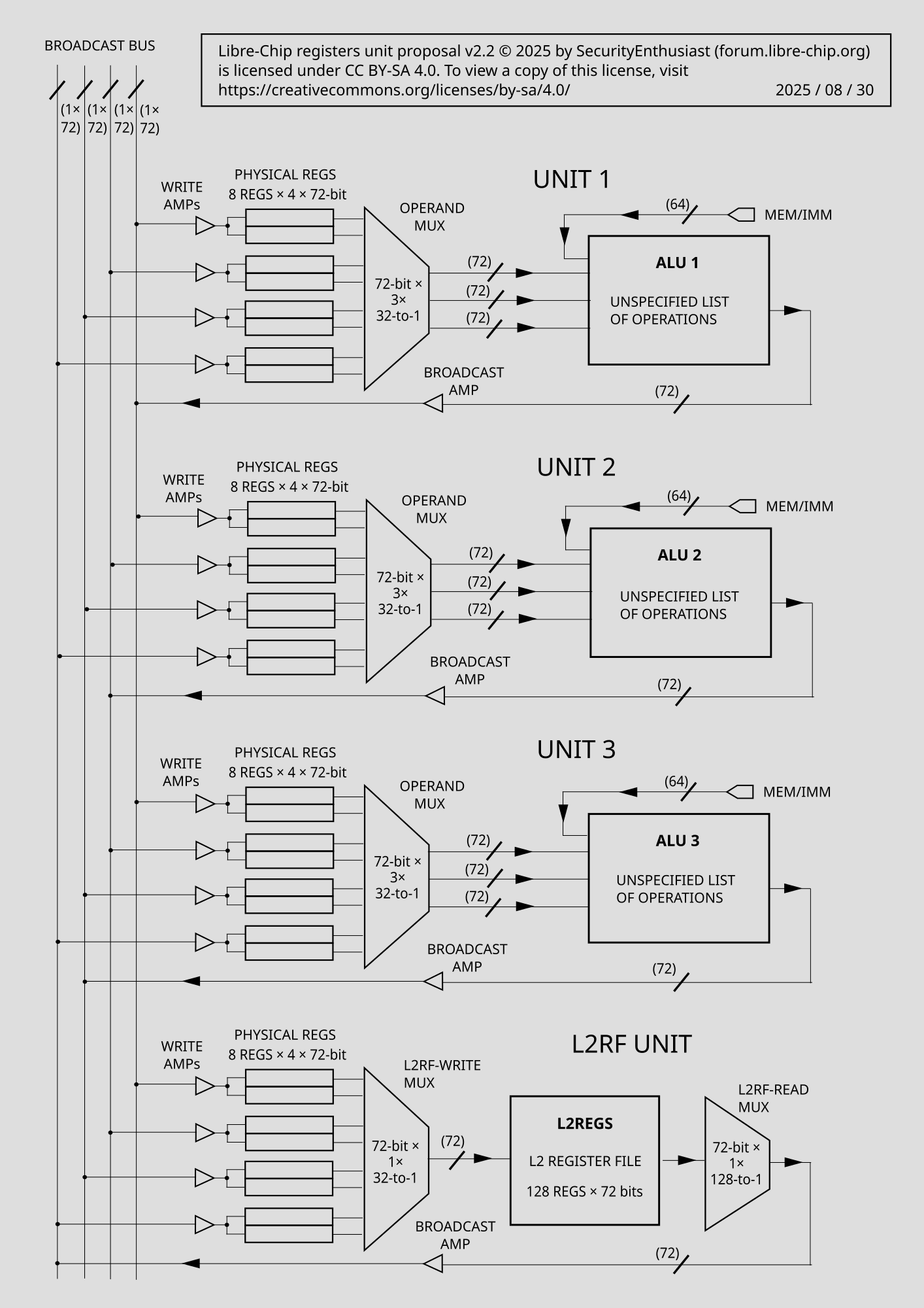
I have drawn a REG-READ unit, so that this schematic completes the drawing of everything attached to the broadcast bus.

If there are any other units on the broadcast bus, then they should be added to this schematic. But, I couldn't think of any on top of my head.

Post comments regarding errors in the drawing, or suggested changes.

EDIT: I have just figured out that this REG-READ unit also needs physical registers... Uhh. I'll try to see how to fix that.

  • Fixed the REG-READ unit schematic.

If there are any other units on the broadcast bus, then they should be added to this schematic. But, I couldn't think of any on top of my head.

Post comments regarding errors in the drawing, or suggested changes.

I think we drifted off topic.

I would like to reserve this thread for comments related to my original "High-performance execution unit" proposal (the one that enables a 20% higher clock rate). The title of this thread refers to that proposal.

I created a new thread for discussion of the current design and for posting drawings of the current Execution Unit.