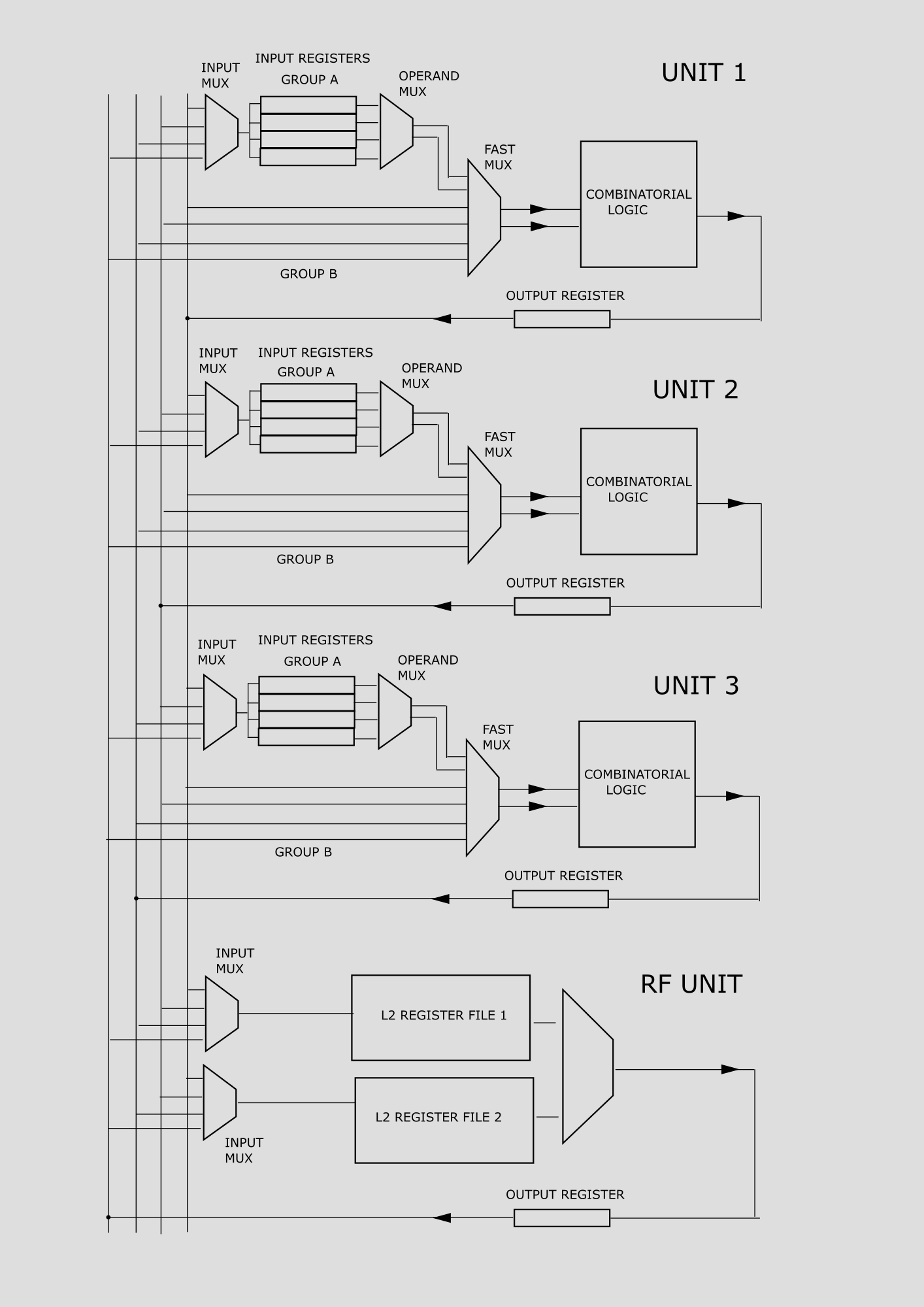
Idea for changing the register file and muxing to make it faster

I must first apologize for commenting all over this forum... you don't need to answer me, I'll just put up some suggestions.

The basic issue with a large set of local (i.e. per-unit) registers is that it is going to waste a lot of time on selecting the register to be red, thereby slowing down the clock rate.

So, I think perhaps a better idea (well, fastest, but perhaps not the easiest) is to have

  • a small number of local output registers (they store results)
  • and a small number of local input registers (they store operands)

A clock cycle ends by a write to local output registers.

The entire trick here is to make the L2 register file have a big write bandwidth (let's say 3 writes per cycle). That ensures the local output registers are mostly free (because their values are quickly copied to L2 registers). Therefore, the number of local output registers is kept low (2 per unit).
Similarly, it can easily be seen that the number of local input registers can be kept to a minimum (i.e. per unit: as many registers as there are units).

I'm just trying to help, hopefully.
I never did a hardware design in my life, I only do software.

I think I’ve found a good compromise that combines your idea (many local input registers) with mine (a small number of local output registers).

Summary

  • Each unit has local input and local output registers.
  • Use 2 local output registers per unit.
  • The output registers are near their unit's output traces. There is no long bus between a unit and its output registers (unlike in your schematic)
  • Each clock cycle ends with a write to a unit’s output registers.
  • All units must have the same number of output registers so their intra-cycle delays stay aligned.
  • Input registers are divided into two groups per unit: Group A and Group B
  • Group A — a large pool of local input registers holding operands received in previous cycles.
  • Group B — a small set of fast pass-through input registers used for recently produced operands forwarded from other units. For each unit, the number of registers in group B equals the number of units (one fast slot per potential producer).
  • The input of each register in group B is connected, over a long bus, to output of one unit's output registers.

Timing balance

  • The goal is to equalize the read delay for operands coming from Group A and Group B so they become available at the same intra-cycle time.
  • Group A requires large multiplexers to select among many stored values.
  • Group B values are forwarded from other units’ output registers and must traverse a long bus, which consumes time.

To match delays, Group B reads use shallower (faster) multiplexing while Group A reads use deeper (slower) multiplexing. The bus traversal latency for Group B is compensated by faster selection logic; Group A’s values don’t pay the bus traversal cost because they were received in earlier cycles.

Why this works

Group A can be large because its operands arrived in previous cycles; they don’t need to travel over the long forwarding bus during the current cycle, so you can tolerate deeper selection logic.

Group B provides a last-moment fast-forward path for recently produced operands.

(EDIT: added schematic image)
(P:S. When I think better about it, Group B doesn't even have to be registers, it could just be directly wired fast-forward. Regarding output registers, there must be at least one per unit, because clock cycle ends at output registers)

having output registers is equivalent to the design I came up with where there's only input registers -- the only difference is that with input registers the broadcast busses are before the registers instead of after, which allows a reduction in the number of broadcast busses for equivalent throughput because you only need one bus per unit instead of having to have one bus per unit's input -- inputs are generally wider than outputs so that reduces wiring requirements without reducing throughput.

What you drew with muxes on the output registers reduces throughput because you can only read one value from each unit per cycle and you can often want to read more than that because the instruction has multiple inputs from the same unit's output.

Also, when combining input registers and output registers, how do you tell when you should move data from an output register to an input register? With only input registers it's easy: every output is always written to input registers.

Also, the way I envisioned the L2 register file is that it's a last resort when you run out of the fast input registers (e.g. you have 12 div instructions in a row but the div unit can only write to 8 different registers, so the CPU inserts copies from 4 of those div unit registers to the L2 register file).
The L2 register file is optimized more for density rather than bandwidth, so has 1 write port and 1 read port.

having output registers is equivalent to the design I came up with where there's only input registers -- the only difference ...

You missed the point. The point is to increase the clock rate. So, in my design (new schematic provided below), the "FAST MUX" is much faster then the equivalent MUX in your design.

The rationale: the clock rate should be set such that the ADD / SUB operation takes 1 cycle. However, the adder / subtractor will use up less than 40% time of a clock cycle. The rest will be lost on the broadcast bus and multiplexing.
By reducing the size of the FAST MUX (therefore providing a fast-forward lane), the clock rate would likely be increased by about 20% in my design.

What you drew with muxes on the output registers reduces throughput because you can only read one value from each unit per cycle and you can often want to read more than that because the instruction has multiple inputs from the same unit's output.

You incorrectly interpreted what I meant.

  • I'm considering only units that can produce one value per cycle. Therefore, there is no point of reading more than one value.
  • If you need units that can produce more than one value per cycle, then such unit might need to have (in the new schematic) two output registers and two bus tracks.

Also, when combining input registers and output registers, how do you tell when you should move data from an output register to an input register? With only input registers it's easy: every output is always written to input registers.

Of course, there is a way to tell, but it is definitively more complicated than in your schematic. But, anyway, the bandwidth is so high and the number of registers in GROUP A can be so large, that in most cases it is safe to default to "move" action in almost every clock cycle for almost every unit.

Also, the way I envisioned the L2 register file is that it's a last resort when you run out of the fast input registers (e.g. you have 12 div instructions in a row but the div unit can only write to 8 different registers, so the CPU inserts copies from 4 of those div unit registers to the L2 register file).
The L2 register file is optimized more for density rather than bandwidth, so has 1 write port and 1 read port.

In my design, it would be much easier if you make the L2 file receive a copy of most of the results. The number of writes to the L2 file can be reduced, but such would add more complexity.

I have updated the schematic by adding more labels.
Also I'm thinking of another improvement: to make each unit have two "input MUXes", instead of only one.

Here, below, I have drawn this alternative variant. Only 4 input registers per unit are drawn, due to space constraints on the image. The total number of input registers should be much higher.

Also, I would guess that a good number of units is 6, with a total of 96 input registers (plus a L2RF unit).

Alternatively, 13 units is also possible, with 104 input registers in total, although it would complicate the design somewhat.

EDIT:
I have another idea. The registers in GROUP A are not speed-sensitive, and the L2RF is also not speed-sensitive. So, why not just use dual-write-ports register files? That would simplify the scheduler somewhat. I don't know whether that is a good idea. Are dual-write-ports register files prohibitively complex for this ALU ?

TL;DR: Dual write ports are not a good idea.

I have been playing with the dual-write-port idea mentioned in the previous post.
It turns out that the timings are too tight, which would require a lot of additional power.
Also, those dual write ports eat up a lot of the transistor budget.

So, my judgment is: better without dual write ports.

Thanks for your effort but I'm most likely not going to change that part of the CPU design now since I do want to get a working CPU design before spending a bunch of effort on speed optimizations that aren't all that necessary at this point.

Maybe you could try implementing your design later once we have a working CPU.

I think we both have potential misunderstandings but I'd rather work on getting a working CPU and actually writing code than spend a lot of effort arguing.

Well, that makes sense because your design is simpler.
I think it is a good idea to start simple.

If you ever want to use my high-performance execution unit which allows for 20% higher clock rate, below are the schematics I made so far, and some of my notes.

	- provided a new schematic for the execution unit, v5.0
	- provided an example schematic for L2RF ALU  (but timings are very tight)
		(Simple ALU unit roughly sketched, as an example)

	- 7 units total (including L2RF unit)
	- proposal for 5 unit types: A, S, M, D, L2RF
	- The Unit type D can now produce two 64-bit results per clock cycle
		- it shares one output register with the L2RF unit
		
	- Tried to assign operations to each unit type (in text below)
		
	- The FO4 gate delays are rough guestimates
		- I need data on gate delays to be able to draw and synchronize the ALUs
		- How may gate delays for:
			- 1 level multiplexer ( 2-to-1)    (assumed 2.3 gd)
			- 2 level multiplexer ( 4-to-1)    (assumed 4.6 gd)
			- 3 level multiplexer ( 8-to-1)    (assumed 6.9 gd)
			- 4 level multiplexer (16-to-1)    (assumed 9.2 gd)
			- from D-latch open to output valid (i.e. latency of registers) (assumed 2 gd)
			- from output register latch open to fast mux   (assumed 9 gd)
			- for each arithmetic / logic operation

FO4 gate delays:			  
	One Clock Cycle:
		   9 gate delays from output register latch open, to FAST MUX
		+  7 gate delays:  fast mux (8 to 1)
		= 16 gate delays from output register latch open, to BIG ALU
		+ 11 gate delays:  combinatorial logic for add/sub/cmp or shift/rot
		= 27 gate delays TOTAL (FO4)	
		
	11 gate delays from output register latch open, to INPUT MUX
	22 gate delays from output register latch open, to INPUT REGS
	  
	Intra-cycle latches timing:
		- input regs  open latches at 0 gate delays (intra-cycle timing)
		-   L2regs    open latches at 2 gate delays (intra-cycle timing)
		- output regs open latches at 5 gate delays (intra-cycle timing)


Unit  1     (Type S):           << Should be the tightest unit regarding max. clock speed
	shift/rot     ( 1 cycle )	   

Units 2, 3  (Type A):           << Should also be the tightest unit regarding max. clock speed
	add/sub/cmp   ( 1 cycle )	
	
Units 4, 5  (Type M):	        << Should not be very tight; if it is, then it should be trimmed	
	mul pipelined ( 4 cycles) line 0 ----=> muxed into line 2
	mul           ( 3 cycles) line 1 ---------------_     
	add/sub/cmp   ( 2 cycles) line 2 --->----|\_     \    _
	shift/rot     ( 2 cycles) line 3 --|\____|/ \     \__| "-_   
	popcnt        ( 2 cycles) line 4 >-|/        \_|\____|    "-.
	leading bits  ( 1 cycle ) line 5 --------------|/    | MUX  |____ to outp. reg.
	inc/dec/abs   ( 1 cycle ) line 6 --------------------|      |    
	sign extend   ( 1 cycle ) line 7 --------|\__________|   _-"
	bitwise       ( 1 cycle ) line 8 --|\____|/          |_-"  
	passthrough   ( 1 cycle ) line 9 --|/
	memory or imm read        line X ----=> muxed into line 4
	
Unit 6      (Type D):           << Should not be very tight; if it is, then it should be trimmed
	div pipelined (38 cycles)        --|\__
	isqrt         (26 cycles)        --|/  \_|\__...----=> muxed into line 2
	mul long      ( 6 cycles)        --------|/ 
    mul           ( 3 cycles) line 1 ---------------_     
	add/sub/cmp   ( 2 cycles) line 2 --->----|\_     \    _
	shift/rot     ( 2 cycles) line 3 --|\____|/ \     \__| "-_   
	popcnt        ( 2 cycles) line 4 >-|/        \_|\____|    "-.
	leading bits  ( 1 cycle ) line 5 --------------|/    | MUX  |____ to outp. reg.
	inc/dec/abs   ( 1 cycle ) line 6 --------------------|      |    
	sign extend   ( 1 cycle ) line 7 --------|\__________|   _-"
	bitwise       ( 1 cycle ) line 8 --|\____|/          |_-"  
	passthrough   ( 1 cycle ) line 9 --|/
	memory or imm read        line X ----=> muxed into line 4

Unit 7      (Type L2RF):       << Should not be very tight;
	L2 registers  ( 1 cycle )
	inc/dec/abs   ( 1 cycle )
	Unit D result ( 1 cycle )
	sign extend   ( 1 cycle )
	passthrough   ( 1 cycle )
	memory or imm read (to output register)

I split this out into a new topic, please don't post on very old topics when you have a new thing to discuss. You can quote (which also links to) whatever message you're referring to.

OK.

So, let’s discuss your execution-unit design in more detail.

You need to map the Power ISA arithmetic and logical instructions to the ALU units. You can follow the same mapping scheme I used in my design.

Could you post an overview showing how you intend to map arithmetic and logical operations to each ALU unit in your design,
as I did in my previous post?

What do you think about the mapping in my design (details are in the notes given in my previous post):

  • Mapping is organized by unit type.
  • There are five unit types: A, S, M, D, and L2RF.

I have re-drawn your design to make it more clear and readable, and fixed that awful format where the image was too high. The original is from:

I would like to add more details to the schematic of your design:

  • what are the estimated timings for each component on the image ?
  • do you want any changes or additions to the image? Do you want to change or add some labels?
  • will there actually be 3+1 units, or more?
  • the new schematic says "unspecified list of operations" for ALUs of each unit. What is the mapping of operations to units? Are ALUs supposed to be homogeneous or heterogeneous?

EDIT: How are memory reads performed in your design? It is not clear from the schematics how is data from memory reads inserted into the register unit. Is it the same way as in my Unit L2RF (or Unit Type M, the same)?

Here is my re-draw first, then the original design of yours:

I do want to get a working CPU design before spending a bunch of effort on speed optimizations that aren't all that necessary at this point.

OK, let’s focus only on optimizations that simplify your design.

Gate-delay estimates are essential for any high-performance design.
You can't do a meaningful design without timings — and especially a high-performance design.

As I understand it, Libre Chip ultimately targets both FPGAs and custom silicon.
I’ll primarily optimize for custom silicon; most conclusions should still apply to FPGAs.

I computed gate delays using the logical-effort method, and found my earlier guesses were off.
I computed delays for a 14 nm process or better (valid down to ~5 nm).

For your design (per my drawing), (3+1) units, the delays are:

	    3.0 FO4  input amplifier delay for operand registers
	    1.0 FO4  operand register passthrough delay
	    4.8 FO4  operand mux delay
	   11.0 FO4  ALU delay (assuming the 3+1 units case)
	    1.0 FO4  broadcast-bus amplifier delay
	    1.5 FO4  broadcast-bus length delay (I'm not very certain about this value)
	 = 22.3 FO4  = one clock cycle TOTAL

At 7 nm process, you would get 1 FO4 = 11 ps (at high voltage).
So the max clock rate of your design at 7 nm is: 1 / (11 ps) / 22.3 = 4.08 GHz

The optimization question is: what is the optimal number of operand registers per unit?
The table above assumes 64 operand registers per unit.

Recomputing for 32 operand registers per unit:

	    2.5 FO4  input amplifier delay for operand registers
	    1.0 FO4  operand register passthrough delay
	    4.0 FO4  operand mux delay
	   11.0 FO4  ALU delay (assuming the 3+1 units case)
	    1.0 FO4  broadcast-bus amplifier delay
	    1.5 FO4  broadcast-bus length delay (I'm not very certain about this value)
	 = 21.0 FO4  = one clock cycle TOTAL

Max. clock rate with 32 operand registers at 7 nm: 1 / (11 ps) / 21 = 4.33 GHz

That is a 6% speed increase, which is unlikely to be offset by halving the number of registers to 32.
Those registers also consume significant die area and transistor budget.
My recommendation is to use 32 operand registers per unit — a slightly faster and more area-efficient alternative to 64. But the speed benefit is small, I think.

I can update the schematic so the L2RF unit can write two values per cycle to 2 banks of L2REGS, if you want.

The next optimization is the number of units: (3+1) or (6+1) ?
I'll do that computation later.

Can you provide the delay numbers for the FPGA target so I can optimize that case?

Currently the registers are actually 72-bits: 64-bits of data and 8-bits of flags (though that may change if we need more flags).

The current CPU design is based on parameters that you feed into it when generating the output verilog, so you can easily select a different number of input registers per unit, a different number of units of each kind, and more. I'm thinking of having 8-16 input registers per unit per output from the same/other units, so if there's 4 units that gives 8 * 4 * 4 = 64 input registers in the whole CPU. Those input registers are likely duplicated for different inputs for each unit, so an add-with-carry unit would have 3 inputs (2 data and 1 flag for the carry-in). each set of registers having only one write port and one read port makes them much more efficient, especially on FPGAs where the built-in SRAM blocks only have 2 ports.

Because it's parameterizable (and because it makes the diagram too busy), I decided to leave out input register counts and widths.

I used a diagram that converts to a .svg file because you can scale it to any size and it still looks high-quality (important for zooming in/out and for high-resolution screens such as mobile and 4k). Also that allows you to select and copy text from the diagram, as well as much more easily edit the source .dia file.

The FPGAs we're likely going to use (unless we decide we need bigger ones) are the ECP5 85F-5G (Because Cesar and I already each have a Orangecrab) and the XC7A100TCSG324-1 because I have a Arty A7-100T plugged into the CI server (though I haven't yet gotten around to doing all the software config so it's accessible to CI). We picked those because they work with open-source FPGA toolchains.

Currently the registers are actually 72-bits

This is fixed in the new schematic v2.1 (below).

so if there's 4 units that gives 8 * 4 * 4 = 64 input registers in the whole CPU

Actually, 8 * 4 * 4 = 128.

So, now I'm confused about how many physical operand registers there are.
I removed the "input/output registers" terminology from the schematic because it's confusing in your design (they behave as both input and output).
I renamed them "operand registers" in the new schematic.

The easiest way to communicate the correct number is for you to look at the new schematic and tell me whether you want the number of operand registers halved.

There is another problem with a large number of operand registers per unit (currently 64 operand registers per unit): they require a very large multiplexer, and those are slow on FPGAs.

Estimates:

 +------------+------------------------+-----------------------+
 | Device     | 64 to 1 mux delay (ps) | 64-bit add delay (ps) |
 +------------+------------------------+-----------------------+
 | XC7A100T   | 5,000–6,000            | 2,000–3,000           |
 | ECP5-85F   | 4,000–8,000            | 2,500–4,000           |
 +------------+------------------------+-----------------------+

So I recommend halving the current number of registers per unit.
I think you were suggesting halving it twice — that would be tight but probably OK.

If you halve the number of registers, I strongly recommend splitting L2REGS into two banks to increase write bandwidth.

Do you want me to apply these changes to the schematic?

I also added memory-read inputs to the schematic, the same way as in my design.
I think that is the best way to add memory reads.

The FPGAs we're likely going to use

Lattice ECP5 85F-5G             ( 57 K LUT6-eq, native 85K LUT4-equivalent)
Xilinx Artix-7 XC7A100TCSG324-1 (100 K LUT6 )  true 6-input LUTs

They are about the right size for a nice OoO speculative CPU.
I guess they can't hold an L3 cache (not important), but L1 cache is important because it must be speculation-aware; L2 can be an ordinary cache.

... continuing the reply....

each set of registers having only one write port and one read port makes them much more efficient, especially on FPGAs where the built-in SRAM blocks only have 2 ports.

Hmm. I would recommend two read ports for operand registers.
Especially if their number is halved.
That won't take up much space. I don't see any problems with dual-read port register files. They will simplify the scheduler and provide more parallelism. It would be a pity not to use dual-port reads.

Also, why not implement operand registers as LUTs? Wouldn't that be much faster?

Anyway, the L2REGS have single read and write ports.

I tried the dual-write port on one of my designs (schematic provided earlier). The next message of mine was:

"Dual write ports are not a good idea."

oops...

I call them input registers because they sit close to the inputs of each unit, after the slow broadcast busses.

the unit has some number of inputs dependent on which instructions it processes, for add-carry it's 3 inputs. each input has its own independent input registers (that always hold the same contents as the input registers for the other inputs).

actually, the LUT-based mux they need is only 4-to-1 for 4 units since there's a FPGA block RAM for each pair of unit input and unit output. that FPGA block RAM has only one output the way we're using it (Pseudo 2-port -- meaning one read-only port and one write-only port) but it can store lots of registers -- on the ECP5 each block RAM is 18kbit (see page 25 of the data sheet), so, since they max out at 36-bits wide we use 2 block RAMs per input/output pair so that's 18kbit*2/72-bit=512 registers per input/output pair, the design uses substantially less than that so the ASIC version isn't too horribly inefficient.

they sneakily have N read ports for a N-input unit, by duplicating them N times so each duplicate only needs 1 read and 1 write port.

Maybe? I'm not sure. We can figure that out later, it shouldn't be that hard to change in the code.

To be clear, if you want to make a new image to replace the one on the website, please use a format that ends up as SVG and submit the original source file if that's something other than SVG. You can submit a PR here. I have it translate the .dia file to .svg in CI which is used to build the website from markdown using mdBook.

Note the website is licensed under LGPL-2.1-or-later OR LGPL-3.0-or-later so it allows us to easily copy/move content between the website and the other repos.

the unit has some number of inputs dependent on which instructions it processes

That phrasing is confusing.

When discussing the register unit (which is the topic here), the only relevant inputs are register operands.
Flags, immediates, and other instruction fields are "aside inputs" and should not be counted as operands.

Instructions have either zero, one or two input register operands.
I believe the Power ISA has no three input register-operand instructions.
Therefore, each ALU unit can accept at most two register-operand inputs, and that is clearly shown on my schematic.

the unit has some number of inputs dependent on which instructions it processes

Well, that is true, but also it is also a completely irrelevant and obvious "always-truth".
Also true: Each ALU unit always has the same number of inputs (because inputs are physical wires).
Also true: Each ALU has at most two register-operand inputs (but it is likely that all ALUs will have 2 register-operand inputs because we canot afford a high ALU unit count; the ALU unit count will be either 3+1 or 7+1)

for add-carry it's 3 inputs

For add-carry, it has many other wires as inputs, not just 3 inputs.

For add-carry, it's two register-operand inputs.
That is drawn on my schematic.
I'm not going to draw every single control wire that goes into an ALU in that overview schematic.

I call them input registers because

That terminology is misleading and a poor conceptual fit for your design.
Confusingly, on your original schematic they are called "output registers".
I know there hasn’t been time to standardize terms yet, so let’s do that now.
I used "operand registers"; you may choose a different name if you prefer, but please avoid "input registers" and "output registers."

	In the ISA:                        architectural registers (or architected registers).
	After register renaming:           physical registers (or renamed physical registers).
	duplicate physical registers:      replica registers
	"operand/input/output registers":  ...choose something

they sneakily have N read ports for a N-input unit, by duplicating them N times so each duplicate only needs 1 read and 1 write port.

That's simply called "dual-port read."
That you plan to implement it with replica registers is irrelevant and need not be mentioned.

If a detail about those replica registers is important, explicitly say "replica registers" so it's clear what you mean.
Otherwise, it is just "dual-port read" physical registers, and abstract away their implementation.

To be clear, if you want to make a new image to replace the one on the website, please use a format that ends up as SVG

Yes — I want to create a new image. The original drawing is an SVG composed of lines, triangles, and rectangles.
That image is documentation, so I believe the appropriate license is the GNU FDL. I’ll find out how to apply that license to an image.

You can submit a PR here.

I will not submit it.
I’ll post the images in the forum, and you can submit them to the Git repository if you want.

Those images are basic documentation, and they should be publicly discussed on this forum and easily accessible to anyone on this forum, not just submitted to the GIT where they will be lost in some sub-folder.

One of the project’s major Achilles’ heels is the near-total lack of documentation, and I intend to change that.

That’s why I want us to agree on common terminology so we can communicate more easily.

on the ECP5 each block RAM is 18kbit (see page 25 of the data sheet), so, since they max out at 36-bits wide we use 2 block RAMs per input/output pair so that's 18kbit*2/72-bit=512

OK. But the ECP5 has only about 32 BRAMs. And you pair them into 16 pairs.
That allows max. 16 simultaneous reads, and you are going to use it up for the physical "operand" registers.
I'm not an FPGA expert, I'm just mentioning it, maybe I'm wrong.
It seems to me that those BRAMS could maybe be more useful elsewhere.

Implementing a total of 128 physical "operand" registers as LUTs would use up about 10 K LUTs, I guess.
Add another 6 K for the read MUXes. It is a lot, but not prohibitive.